TSMC's Fab Wafer Capacity breakdown

Taiwan Semiconductor Manufacturing Company (TSMC), the global leader in contract chip manufacturing, stands at the heart of the semiconductor industry, powering everything from smartphones to cutting-edge artificial intelligence systems. The data in this article is from TrendForce.
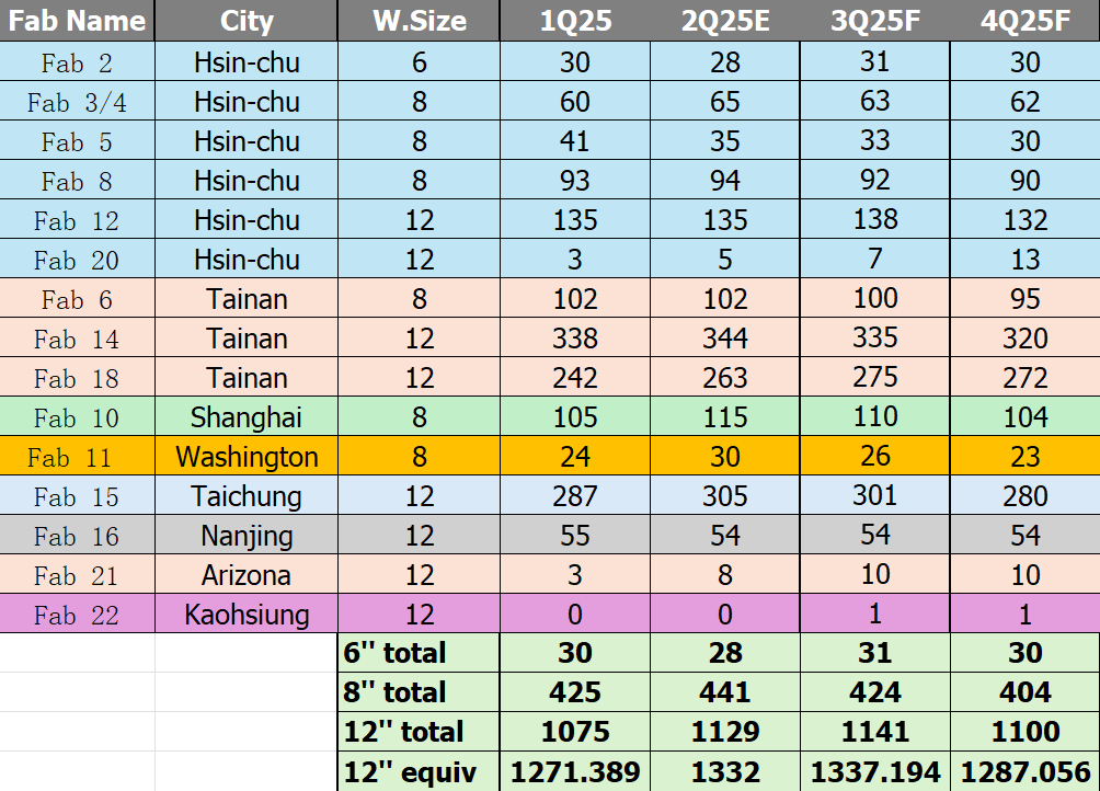
The wafer sizes—6, 8, and 12 inches—reflect TSMC’s diverse manufacturing capabilities. The 12-inch wafer fabs, including Fab 12, Fab 14, Fab 15, Fab 18, Fab 20, and Fab 21, are the backbone of advanced production, supporting nodes as small as 3nm and below, which are critical for high-performance computing and AI applications. Fab 12, for instance, boasts a capacity ranging from 135 WSPM in 1Q25 to 132 WSPM in 4Q25F, a slight decline that could signal planned downtime for equipment upgrades or a shift toward newer facilities like Fab 18, which scales from 242 WSPM to 272 WSPM. This suggests TSMC is strategically reallocating resources to maintain its edge in cutting-edge process technologies, a move likely influenced by competition from rivals like Samsung and Intel.
The 8-inch wafer fabs, such as Fab 2, Fab 3/4, Fab 5, Fab 8, Fab 10, and Fab 11, cater to mature and specialty processes, often used for analog chips, power management ICs, and automotive semiconductors. Fab 8’s capacity grows from 93 WSPM to 90 WSPM, reflecting steady demand, possibly driven by the automotive sector’s increasing reliance on chips for electric vehicles and advanced driver-assistance systems (ADAS). Fab 11, highlighted in yellow, sees a rise from 24 WSPM to 23 WSPM, which may indicate a targeted expansion to support legacy products or a pivot to meet supply chain resilience goals following recent global shortages. The yellow marking could also hint at a strategic investment, potentially backed by government incentives to bolster domestic production amid geopolitical tensions.
The 6-inch wafer fab, Fab 22, with its minimal 0 to 1 WSPM, appears largely phased out or reserved for niche applications, aligning with industry trends favoring larger wafers for cost efficiency and higher yields. The summary rows for wafer sizes tell a compelling story: 12-inch capacity surges from 1,271,389 WSPM in 1Q25 to 1,287,056 WSPM in 4Q25F, underscoring TSMC’s focus on advanced manufacturing. This growth coincides with the rollout of new nodes and the expansion of facilities in Taiwan, the U.S. (e.g., Arizona), and potentially Japan, where TSMC is building fabs to diversify its footprint amid supply chain concerns.
Color-coded categories—new (green), mature (orange), specialty (red), and others (gray)A—add depth to the analysis. The mature fabs, like Fab 10 and Fab 11, show resilience, with Fab 10 increasing from 105 WSPM to 104 WSPM, likely supporting stable demand for older nodes used in industrial and consumer electronics. Specialty fabs, such as Fab 6 and Fab 14, with capacities like 102 WSPM and 338 WSPM respectively, are pivotal for advanced packaging and 3D IC technologies, areas where TSMC is investing heavily to meet the needs of AI and high-bandwidth memory (HBM) chips. The new category, led by Fab 20 with a modest 3 to 13 WSPM, represents emerging capacity that could ramp up as TSMC’s global expansion projects, such as the Arizona Fab 21, come online.
Seasonal and quarterly trends further illuminate TSMC’s strategy. The slight capacity increases from 2Q25E to 4Q25F in fabs like Fab 15 (287 to 280 WSPM) and Fab 18 (242 to 272 WSPM) suggest a ramp-up to meet year-end demand, possibly for holiday electronics or new AI hardware launches. Conversely, stable outputs in fabs like Fab 21 (3 to 10 WSPM) might reflect a cautious approach to new capacity until market conditions solidify. These adjustments align with TSMC’s history of balancing supply with demand, a skill honed through decades of serving clients like Apple, Nvidia, and AMD.
Beyond the numbers, TSMC’s capacity growth reflects broader industry dynamics. The semiconductor shortage of 2021-2022, exacerbated by pandemic disruptions and geopolitical risks, has pushed TSMC to expand aggressively. Its partnerships with governments, including the U.S. CHIPS Act and Taiwan’s subsidies, are likely fueling investments in new and existing fabs. Moreover, the rise of AI and 5G technologies, which demand advanced nodes and high-volume production, positions TSMC to capitalize on these trends. The data also hints at potential challenges, such as workforce scaling and energy demands, which TSMC must address to sustain this growth.
In conclusion, TSMC’s fab capacity data as of June 2025 paints a picture of a company at the forefront of semiconductor innovation, with a clear tilt toward 12-inch wafer production and a strategic mix of mature, specialty, and new facilities. The gradual capacity increases and facility-specific trends suggest a well-orchestrated plan to meet rising global demand while navigating supply chain complexities. As TSMC continues to expand its global presence and technological prowess, this analysis offers a window into its operational strength and its critical role in shaping the future of technology.