Talk about CXMT

According to news from Chinese securities firms, CXMT is launching IPO counseling to prepare for its IPO. We will talk about CMXT in this post.
Roadmap
According to a research report by Morgan Stanley, CXMT plans to start mass production of HBM2E in the first half of 2026. This progress marks its breakthrough in the HBM field, especially against the backdrop of growing demand for AI and high-performance computing. It is expected to achieve small-scale mass production by mid-2025, gradually transitioning to full mass production.
Regarding HBM3, South Korean media Financial News reported that CXMT plans to deliver HBM3 samples by the end of 2025 and is expected to start full-scale mass production from 2026. A further goal is to develop the fifth-generation HBM (HBM3E) in 2027, aiming to narrow the technological gap with international giants such as Samsung, SK Hynix, and Micron.

CXMT’s advanced packaging partners include Tongfu Microelectronics, Changdian Technology, and Jinhua Integrated Circuit, and these partnerships are crucial to its HBM production. For instance, Tongfu Microelectronics provides support in HBM's TSV (Through-Silicon Via) technology and KGSD (bonding technology), enhancing the performance and reliability of HBM2.
Production capacity
According to Morgan Stanley, CXMT's HBM production capacity will reach approximately 10,000 wpm by the end of 2026 and expand to 40,000 wpm by the end of 2028. This growth target reflects its response to the demand in the AI market. However, the global HBM production capacity is expected to reach 340,000 wpm by the end of 2025, so CXMT still has ample room for development.
In the DRAM field, CMXT plans to increase its DDR5/LPDDR5 production capacity to 110,000 wpm by the end of 2025, accounting for 6% of the global DRAM production capacity. Among them, 5,000 to 10,000 wpm of G3 capacity is dedicated to GigaDevice Semiconductor, and the remaining 160,000 to 165,000 wpm is used for LPDDR4x and HBM research and development. In the long run, its production capacity may further expand to over 300,000 wpm (180,000 wpm at the Hefei factory and 120,000 wpm at the Beijing factory).
In 2025, CXMT’s DRAM chip output is expected to account for approximately 14% of the global total, but due to yield issues, its actual market share may drop to 10%.
Technology
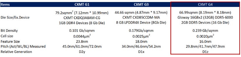
CXMT may face significant challenges in developing the D1 node without using EUV lithography, which could present as obstacles in improving yield, reducing chip size, and scaling up production. Analyses by TechInsights show that CXMT has been able to manufacture DDR5 chips on the 1z nm node, but the die size is relatively large and the yield has not yet been fully verified.
CXMT's goal may be to replicate Micron's 1α nm DRAM developed without EUV lithography, a strategy that would provide experience for its HBM3E development.
Recently, CXMT launched a 16Gb DDR5 chip using the 16nm node, which is approximately 20% smaller than its current 18nm third-generation DRAM. In comparison, the three major DRAM manufacturers currently produce chips with sizes of 12-14nm for 1a/b nm DDR5 production. Based on the mainstream DRAM production of DDR5 16Gb in 2021, CXMT is currently lagging behind by about 3 years. However, its G4 is similar to 1z nm DDR5, and it may target the server DRAM market in the future.