Decoding TSMC's Advanced Process Roadmap: From 3nm Expansion to 1.4nm Mass Production
As the global leader in chip manufacturing, TSMC’s every move shapes the trajectory of the semiconductor industry. From the accelerated expansion of 3nm process to the mass production sprint of 2nm, coupled with adjustments to its overseas factory layout, TSMC’s strategic initiatives have far-reaching implications for the entire supply chain. Based on an expert interview published by Third Bridge, this article comprehensively deciphers TSMC’s capacity blueprint and future trends, offering an in-depth look into the high-stakes race for advanced process dominance.
I. 3nm Process Node: Explosive Demand Growth Drives Beyond-Expectation Capacity Breakthroughs
1. Current Capacity Status: Targets Achieved Ahead of Schedule, Marching Toward 200,000 Wafers
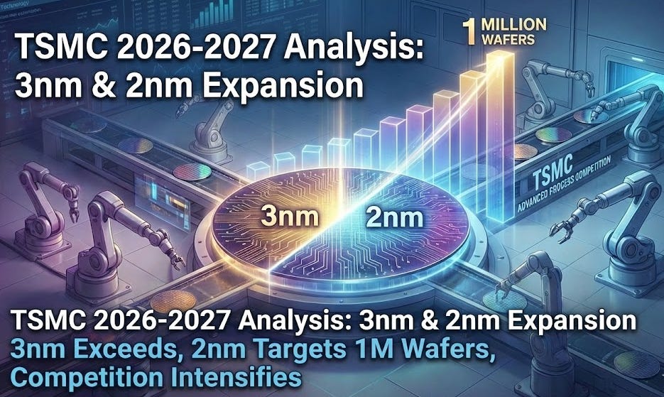
The capacity expansion progress of TSMC’s 3nm process has completely exceeded prior industry expectations. As early as the end of 2025, 3nm monthly capacity had already surpassed 150,000 wafers, hitting the preset target. As of 2026, expansion continues to accelerate, primarily driven by the continuous production ramp-up in the P7 and P8 phases of Fab 18B. Based on TSMC’s standard capacity of 25,000 wafers per phase, the full-scale operation of all 8 phases (P1–P8) at Fab 18B will deliver a monthly capacity of 200,000 wafers. Aligned with the current expansion pace and equipment installation progress, TSMC’s 3nm monthly capacity is highly likely to reach the 180,000–200,000 wafer range by the end of 2026, with potential to exceed this threshold.
Behind this rapid capacity expansion lies explosive market demand, stemming mainly from two core segments. First, the sustained boom in the AI industry: as a leading AI chipmaker, NVIDIA has an urgent demand for 3nm capacity, with order volumes climbing steadily to become the backbone of 3nm demand. Second, the high-end consumer electronics and chip market: major industry players including Apple (for its iPhone 17 series and M-series Mac chips), Qualcomm, MediaTek, and Intel have all placed substantial orders. The convergence of these multiple demand streams has kept 3nm capacity in a state of chronic supply shortage.
2. New Pathways for Capacity Utilization: Retrofits of Existing Fabs Unlock Incremental Output
Beyond building new fabs, TSMC is further tapping into 3nm capacity potential by retrofitting existing facilities. Fab 15B in the Central Taiwan Science Park (CTSP), originally focused on 5nm, 6nm, and 7nm production, had maintained a capacity utilization rate of around 70% for a long time. However, starting from the end of Q4 2025, Fab 15B’s capacity has ramped up rapidly and now operates at full load, with a stable daily wafer output of 4,500–5,000 units.
To accommodate the surging 3nm orders, TSMC launched a process conversion project at Fab 15B: by repurposing part of the existing space and installing 3nm production equipment, the fab aims to add an additional 25,000-wafer monthly capacity (equivalent to one phase) within a year. A key advantage of this retrofit approach is that it leverages Fab 15B’s existing workforce and cleanroom infrastructure, eliminating the need for greenfield construction and significantly shortening the capacity ramp-up cycle. Including this incremental capacity, TSMC’s total 3nm monthly capacity in Taiwan is expected to exceed 200,000 wafers by the end of 2026, potentially reaching an above-expectation level of 220,000 wafers.
Notably, an interesting trend has emerged in Fab 15B’s capacity dynamics: the backend processes for 5nm and 3nm share certain equipment, leading to the transfer of some orders originally produced at other fabs to Fab 15B. Meanwhile, demand for 6nm and 7nm processes has seen a marked uptick recently. While the exact source of this demand remains unclear (it may span areas such as Bitcoin mining chips, automotive electronics, and consumer electronics), this shift has further boosted Fab 15B’s capacity utilization rate, freeing up more space for the 3nm conversion project.
3. Future Expansion Plans: 50,000-Wafer Increment in 2027, New Phases to Follow in 2028
TSMC’s roadmap for 3nm expansion remains clear. Phase 9, the subsequent expansion phase of Fab 18B, has completed construction planning and is expected to enter the equipment installation phase in Q1 2027, with mass production slated for late Q2 2027 at the earliest. Following TSMC’s typical capacity ramp-up timeline, this phase will achieve full production of 25,000 wafers per month within one year.
Combined with the 25,000-wafer incremental capacity from the Fab 15B retrofit, TSMC’s total 3nm monthly capacity will increase by 50,000 wafers in 2027, rising from 200,000 wafers in 2026 to 250,000 wafers. Additionally, TSMC has planned three more phases—Phase 10, 11, and 12: Phase 10 will be located adjacent to Phase 9 in the same fab complex; Phase 11 and 12 will be built in the Shalun area on the outskirts of the Southern Taiwan Science Park (STSP), a result of active efforts by the Tainan City Government to attract the project. However, mass production for these three phases is likely to be delayed until 2028, primarily due to TSMC’s current manpower constraints and the need to prioritize the expansion of more advanced nodes such as 2nm, making it difficult to support the simultaneous construction and mass production of multiple new phases in the short term.
If Phase 10, 11, and 12 enter mass production smoothly in 2028, TSMC’s total 3nm monthly capacity will add another 70,000–80,000 wafers (based on ~25,000 wafers per phase), potentially surpassing 300,000 wafers. It is worth noting that the process planning for these three phases retains flexibility: given the high equipment compatibility between 3nm and 2nm, if demand for 2nm grows more rapidly in the future, some of these phases may be converted to 2nm capacity, with adjustments to be made dynamically based on market demand.
II. 2nm Process Node: Mass Production Accelerates Toward 1 Million Wafers in 2026, with 1.6nm/1.4nm Iterations on the Horizon
